Comparison
between FET & BJT


FET symbols

FET is a Field Effect Transistor.
|
BJT
is Bi-polar Junction Transistor.
|
F
ET does not suffer from minority carrier storage effects.
|
BJT
suffers from minority carrier storage effects.
|
FET
is a uni polar device. i.e the current conduction due to majority charge
carriers only.
|
BJT
is a Bi polar device. i.e The current conduction is due to majority and minority
charge carriers.
|
FET has no junctions.
|
BJT
has two junctions.
|
There
are two types of FET’s .
They are 1. N-Channel FET
2.
P-Channel FET
|
There
are two types of Transistors. They are
1. N-P-N Transistor.
2.
P-N-P Transistor.
|
FET has very high input resistance
( i.e 100MΩ ) .
|
BJT
has very low input impedance.
|
The
noise level in a FET is comparatively lower than that in a BJT.
|
The noise level of BJT is high , when
compared t FET.
|
FET amplifiers have low
gain band width Product.
|
BJT
amplifiers have high gain band width product , when compared to FET.
|
FET
is a Voltage-Controlled device.
|
BJT
is a Current-Controlled device.
|
It
has a negative temperature co-efficient at high current levels.
|
It has a positive temperature co-efficient
at high current levels.
|
FET’s are much easier to fabricate .
|
BJT
is not much suitable than FET to fabricate in IC’s.
|
They
occupy less space than BJT.
|
BJT
occupy more space than FET.
|
FET
has higher switching speeds and cut-off frequencies.
|
BJT has lower switching speed and cut-off
frequencies.
|
FET is used as a buffer, RF amplifier, TV
receivers, oscillator circuits, digital circuits etc….
|
BJT
is used as a switches, amplifiers, communication, digital circuits,
oscillator circuits, buffers etc…….
|


E-MOSFET
|
D-MOSFET
|
This
will work with positive Gate Voltage
|
This
will work with negative and zero gate voltage
|
At
zero gate voltage the channel conductance is zero. i.e There is no conducting
path.
|
At
zero gate voltage, the channel conducting path is exist.
|
At
zero gate voltage, ID=0 which is independent of VDS.
|
At
zero gate voltage, ID has some value, this value depends upon VDS
|
Minimum
threshold voltage is needed for the flow of drain current to start.
|
Depletion
MOSFET conducts at 0 volt.
|
In
symbol there will be a broken channel between S to D terminals. There is no
channel in this type to conduct.
|
In
symbol there will be no broken channel between S to D terminals. There is a
channel in this type to Conduct.
|
It
prefers positive voltage to conduct.
|
It less prefers positive voltage to conduct.
|
It
contains leakage current
|
It does not have any kind of leakage
current.
|
Its
operations are opposite to Depletion MOSFET
|
Its
operations are opposite to Enhancement MOSFET
|
In
enhancement MOSFET ,channel does not exist initially and is created by
applying a voltage to Gate terminal.
|
In
depletion MOSFET, channel is fabricated permanently at the time of construction
of MOSFET.
|
Normally known as OFF transistors.
|
Normally known as ON transistors.
|
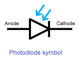


PHOTO TRANSISTOR
Photo diode
|
Photo transistor
|
It
is more responsive to incident light than photo transistor.
|
It
is not as more responsive to incident light than photo diode.
|
It
has more linear response than photo transistor
|
It
has not more linear response than photo diode.
|
It
passes less current.
|
It
passes more current than photo diode.
|
It
consumes more less current.
|
It
consumes more current than photo diode.
|
Less
dark current than photo transistor.
|
Higher dark current than photo diode.
|
It can
be constructed by a reverse bias P-N junction diode.
|
It
can be constructed by BJT or FET
|
It
is used in light detectors, demodulators and encoders.
|
It
is used as light sensitive device, light measurement, opto-coupler.
|
Less sensitivity and its output response is fast
|
More sensitivity and its output response is slow.
|
| It is used for light operated switches | It is used in light detection systems |
| It generates current | It generates current and voltage |
LED
|
LCD
|
LED means light emitting diode
| LCD means liquid crystal device |
Requires high
power. So used for external interface circuit, when driven from IC’s.
|
Can be driven
directly from IC-Chips.
|
Good brightness
level.
|
Moderate brightness
level.
|
Operating Temp
range is -40 to 850C
|
Operating Temp range
is -20 to 600C.
|
Life time is nearly
[20 years (or) 1,00,000 Hrs]
|
Life time is
limited [50,000 Hrs]
|
Emits light in red,
orange, yellow, green, blue& white
|
Invisible in
darkness requires external illumination.
|
Response time is 50
to 500 ns
|
Has a slow decay
time response time is 50 to 200 ms
|
Viewing angle 1500
|
Viewing angle 1000
|
Operating voltage
range is 1.5 to 5 V d.c
|
Operating voltage
range is 3 to 20V A.C
|
Used in shop
watches, Display devices, all toys, T.V & Computer Screens.
|
Used in Display
devices Eg:- T.V & Computer Screens.
|
Designed by S.C
device.
|
Designed by liquid
Crystal material.
|
Consumes more power
|
Essentially acts as
a capacitor & consumes very less power
|
They are small in
size and light in weight.
|
They are large in
size
|
They can be
switched ON & OFF at a fast speed.
|
They can be
switched ON & OFF are quite large time.
|
It requires 10-250
m W power per digit.
|
It requires 10-200 µW
power per digit.
|
Hi good evening madam. Thank you so much for the notes on comparisions between the devices madam. It is very helpful for us madam
ReplyDeleteyou are clear my mind actually after reading your article i got clear my complete doubt. thanks for such easy understanding post. I also got some similar at here just for your info i post here link may be useful for future aspect difference between enhancement and depletion type mosfet
ReplyDeleteFETs (Field-Effect Transistors) are voltage-Hosting Raja controlled devices with high input impedance, while BJTs (Bipolar Junction Transistors) are current-controlled devices with lower input impedance.
ReplyDelete